MIPS Multi-Core Processor and Memory Model Simulator
A C++ program which acts as a simulator for MIPS Assembly Language Programs.
Table of Contents
Usage Instructions
To compile, clone the repo and run make all in the root of the repo. An executable named mips_pms will be created. For running the program, execute it like so:
./mips_pms <no_of_cores> <path_to_program1> <path_to_program2> ... <path_to_programn> [simulation_time](optional) <row_access_delay> <col_access_delay> <print_mode> <block_mode>
Parameters:
no_of_cores: The number of programs you want to execute, i.e., the number of cores in the multi-core simulator. Bounded byMAX_CPU_CORESdefined inconstants.h(currently set to 8).path_to_programi, $1 \leq i \leq \text{no of cores}$ : The path to the MIPS Aseembly program you want core i to execute.simulation_time: If you provide this parameter, then the simulation will only be done forsimulation_timecycles, even if all programs have not been executed till then. The system will stop after those many cycles, and display the usual output containing intermediate state at that time. If not provided, execution is done until all programs have finished.row_access_delayandcol_access_delay: These are the parameters of the DRAM Model in the simulator. Depending on these, the clock cycle delays for various DRAM Activites (row activation, writeback, row buffer writes/reads) are determined. Row Access Delay is the latency (in number of clock cycles) of a row activation and a row writeback. Col Access Delay is the latency in reading data from and writing data to the row buffer. There are other DRAM timing constraints in reality however they have not been modelled.print_mode: If this is set to 0, the program prints out only summary statistics for each core, like number of clock cycles, instruction wise execution count, register contents etc. If set to 1, it prints out the activity in the system at each clock cycle. This includes when requests are issued by each core to the MRM, what requests the scheduler selects from available ones, all DRAM Activity like writeback and row activation, as well as register and memory location modifications.block_mode: If set to 1, it operates the DRAM Memory in non-blocking mode. If it is set to 0, DRAM operates in blocking mode, i.e., the cores cannot move forward while they have a request pending in the DRAM. We recommend to set it to 1 so that optimisations through reordering are possible.
Features
- Structural Similarity: The program has been designed by putting together logically distinct components such as the Memory, Memory Request Manager, and the Processor, and classes are used where required for separation of concerns. The flow of data and control signals between these 3 components has been designed to mimic real hardware designs.
- Algorithmic Similarity: We have tried to keep our high level code feasible to implement in terms of hardware. The program parses, encodes and stores instructions in memory first. It then fetches instructions from memory (using a program counter), decodes them and executes them.
- Memory Latency and Timing Characteristics: The program simulates a DRAM Memory, with appropriate clock cycle delays for writeback, row activation and read/write operations. Moreover, there is an option of running the memory in blocking or non-blocking mode. We also print summary statistics for each core including the number of clock cycles taken, number of times each instruction was executed and the CPI. Also, an estimate of the delay in our Memory Request Manager algorithm has been included in the clock cycle analysis.
- Memory Request Scheduling: We have implemented the First-Ready, First-Come-First-Service (FR-FCFS) Memory Scheduling algorithm as part of the memory manager. We have also encoded data dependencies between instructions to ensure that the semantics of the program is preserved. Moreover, the hardware feasibility of implementing this algorithm has been discussed in our design document, along with a rough estimate of the delay caused by implementing this. This helps to achieve our goal of maximizing throughput of the entire system.
- sw-lw Forwarding: We have implemented sw-lw forwarding, which eliminates the requirement of a memory access for a lw instruction. Due to this, forwarding is given the highest priority. The Memory Request Manager first checks for instructions with forwarded values, and checks for row hits only if no such instruction is found.
- Multi-Core Functionality: The program can handle multiple MIPS Programs running at the same time. The memory request manager keeps track of each core’s requests and is the interface between the cores and the DRAM Memory. There is a finite size Request Buffer, and scheduling algorithms do the job of arbitrating between different requests (from same and different cores). We were concerned purely with maximizing throughput here, which is why we used the FR-FCFS Scheduling algorithm. There are however more interesting approaches which take into account fairness among different cores and/or criticality of processes.
- Detailed Output For Analysis: We print out summary statistics for each core, which includes the number of clock cycles, number of times each instruction was executed, and the CPI. The contents of the entire register file are printed, as well as the contents of all accessed DRAM Memory Locations. Also, the user has an option to print out the activity in each clock cycle. This method gives a detailed view into the inner workings of the system, including the execution of instructions, the requests issued by the processor to the DRAM, the activity like writeback, row activation and Memory Location modification inside the DRAM, and the completion of DRAM Requests.
- Testing Illustration: In the last section on Testing Strategy, we have explained how and in what cases our scheduling algorithm works well, and included those testcases in the repo as well.
This can be a useful tool to analyze multiple MIPS Assembly Language programs and their performance while running.
Architecture Diagrams
This figure illustrates the high-level structure of the system, with the memory request manager acting as an interface between multiple CPU Cores and the DRAM Memory.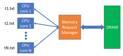
If we zoom into the DRAM Memory, on most modern systems it looks something like the following figure taken from [Rixner00]. Note that we have not considered multiple banks and have limited our analysis to a single bank in the interest of time, however most timing and resource considerations are still there.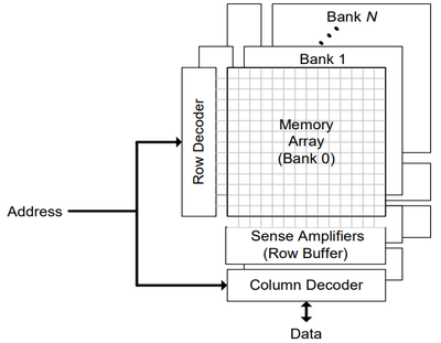
Design Characteristics
- Instruction buffer used by the MRM is of a fixed size. Also, most scheduling operations can be parallelized. These two simple observations allow a hardware implementation such that the MRM can perform scheduling in one clock cycle itself.
- Memory is divided between the cores and each CPU core can only access/modify a part of the total memory. The instruction buffer in the MRM has also been divided into separate sections, so that all the cores can write instructions into the buffer in parallel. This allows the MRM to service all CPU cores in the same clock cycle.
- We have used aggressive reordering, where row hits are given the highest priority. For ordering between multiple row hits and row misses, we have used the FR-FCFS scheduling policy, first introduced in [Rixner00], where the oldest instruction in the buffer is chosen. Since sw-lw forwarding leads to a reduction of memory access, instructions using forwarded values are given a higher priority over row-hits.
Tradeoffs
- Instruction Buffer Size A larger instruction buffer will lead to better reordering decisions. However, it will lead to a higher hardware cost and higher latency. We have currently taken a buffer size (per core) of 32 instructions in the buffer.
Approach of Solution
In the current assignment, the main scheduling (reordering) is done by the MRM, while the DRAM only services requests sent by the MRM. The MRM maintains a buffer of pending memory-access instructions and decides which instruction should be serviced next by the DRAM. The process is explained further in the next section.
Memory Request Manager
For every instruction that requires memory access, we create an instruction object having its core number, target, address, id and an array of dependencies. In this dependencies array, the locations corresponding to other instructions are set to 1 or 0 depending on whether they need to be executed before the current instruction can be considered safe to run. If the instruction stored at index i in the buffer has a data dependency with the instruction to be added, dependencies[i] is set to 1. Every time we add a new instruction to our MRM buffer, we first check for conflicts and set the dependent instructions in the new instruction’s dependencies. Again, when an instruction gets executed, we iterate over all pending instructions and update their dependencies. An instruction is safe to execute if and only if its dependencies array has all zeroes.
While scheduling the next instruction for DRAM to service, the MRM uses an aggressive reordering algorithm, where all instructions with row-hits are executed even if the buffer has older instructions. For ordering between multiple row hits and row misses, we have used the FR-FCFS scheduling policy, first introduced in [Rixner00], where the oldest instruction in the buffer is chosen.
We have implemented sw-lw forwarding. As this forwarding leads to an elimination of memory access in the lw instruction, forwarding is given the highest priority. The MRM first checks for instructions with forwarded values, and checks for row hits only if no such instruction is found.
Multi-Core Functionality
For processing multiple cores in parallel, we initialise multiple interpreter objects, one for each program file given as input. We initialise a single shared MRM that is used by all the interpreter objects. The interpreter objects themselves do not have complete access to the DRAM, and have to interface with the MRM for any memory access. Note that the instruction memory is a separate memory space, that is not shared across multiple cpu cores (interpreter objects).
Although the DRAM memory is shared across the cpu cores, each core is statically assigned its own memory space and any core trying to access memory outside of this allocated space is flagged with an error. The registers are also maintained separately.
The instruction buffer in the MRM is also partitioned, with different cores adding instructions to different locations in the buffer. This partitioning policy allows us to parallelize the process of adding an instruction into the buffer. While executing the instruction, all the cores can add their corresponding instructions to the row buffer in the same clock cycle. This further optimises the MRM.
Hardware Implementation
We have implemented the MRM to most efficiently utilise the parallelism offered by the use of multiple cores. The algorithm used for scheduling is intelligent enough to give optimsed performance, but is also simple enough to be easily implementable in hardware and to be completed in one clock cycle.
For each instructions in the buffer, we first have its index. As the buffer size is fixed (currently 32), the index is stored in a fixed number of bits (currently 5). Then each of the dependencies is stored as a bit-mapped number (again from 0-31, so 5-bit). While adding an instruction, a combinational circuit checks for conflicts with all the instructions in parallel. Since the instructions in the buffer are independent of each other, operating on all of them parallely will not lead to any errors. Again, when an instruction is removed from the buffer, the bit corresponding to its index is simply set to 0 for all the other instructions. In addition to these bits, we have a valid/invalid bit such that if it is set to 0, then the instruction is actually empty (the MRM does not use such instructions in its processing).
Other than these, each of the instruction has with it some priority bits stored. The priorities of different scheduling parameters (eg. row hit, time) are encoded in accordance with their relative order of preference. Since forwarding has the highest preference, the most significant bit stores whether the instruction is being forwarded. After this, the next bit stores whether the instruction is a row hit or a row miss, and finally the last few significant bits store the temporal order in which the instructions were added to the buffer. The priority bits are then sent to a priority encoder, and this priority encoder selects which instruction is to be sent to DRAM next.
The instruction buffer is partitioned so that each core has a separate space where they can add instructions. In hardware, this can be implemented with n (maximum allowed cpu cores) separate write lines (busses), and each line is granted access only some portion of the buffer. As multiple cores cannot write to the same buffer index, there will be no write conflicts. This allows us to parallelize the process of all the cores adding their instructions into the MRM buffer.
MRM Delay Estimation
As discussed in the previous section, most of the processing required for scheduling in the MRM occur in parallel. As the size of the buffer is fixed, a fixed circuit can be implemented that processes all the instructions at the same time. We can implement a priority encoder which has a depth bounded by $log_{2}n$, where $n$ is the number of entries it compares. Since our buffer size is capped at 32, this means a critical path of maximum 5 MUX gates. Assuming 5 MUX gates can run in one cycle, this entire operation can be completed in one clock cycle.Thus, the entire scheduling takes a single clock cycle.
Again, the buffer is partitioned across the cores. So all cores can write to the instruction buffer simultaneously. Thus, the writing to buffer, i.e. interface between cores and the MRM, takes another clock cycle.
During the clock cycle in which MRM performs scheduling, it also sends to the DRAM, the relevant data about which instruction is to be executed next. The DRAM receives this instruction in the edge after the same clock cycle in which the MRM was performing scheduling, and the DRAM can start performing its activities (writeback, copy to buffer etc) from the subsequent clock cycle.
Thus, the MRM effectively requires only two clock cycles. After the end of the second clock cycle, (i.e. in the third clock cycle), the DRAM starts performing the required activities corresponding to the instruction it received from the MRM.
Testing Strategy
The test cases are written as separate files inside relevant folders inside the main directory testcases. The testing has been divided into the following subcategories and test cases of each have been checked to ensure correct working of our interpreter.
1. Reordering
Here, we consider test cases where aggressively reordering significantly improves performance over the first-come first-serve scheduling policy.
We consider one testcase which is a long stream of load word instructions. We believe this emulates a scenario where a program copies 2 different arrays but only uses one loop for that. Both those arrays occupy different rows of the DRAM. Without an aggressive reordering policy, this would lead to 3 writebacks every iteration, since we have a stream of load word instructions with rows alternating.
The second testcase has a loop, in which we have 2 load word instructions to different rows, and a store word instruction as well to a different row. Since these are large numbers of memory requests. but they go to different rows, not reordering them would cost a lot of cycles. This case specifically also shows that the handling of writes is integrated with the handling of reads, and works fine. It also contains a mechanism to check that the value being stored in every iteration is the correct one, to check that reordering doesn’t change the semantics of the program.
2. SW-LW Forwarding
This testcase shows the significant improvement on performance that sw-lw forwarding has. The testcase consists of a loop, and in every iteration we have a lw instruction, on whose value the next addi instruction is dependent. We also have a sw instruction at the end of each iteration, to the same address as the lw at the beginning of the next iteration. This can be a very typical case for programs, because we are just fetching a value from memory, performing some computations with it, and then storing the result to the next block of memory iteratively. Since we have implemented sw-lw forwarding, the lw instruction at the beginning doesn’t have to wait for the sw instruction before it to finish. This not only reduces the number of cycles the DRAM is working for (also decreasing power consumption), but crucially, prevents the next addi from being stalled for a long time. This enables the processor also to keep moving and thus exploits the ability to run DRAM and processor in parallel.
3. Syntax Errors
We had made the interpreter robust towards syntax errors in the input MIPS program. The syntax errors are flagged and appropriate error messages are displayed on the terminal. We have handled the following syntax errors:
- Unrecognized command.
- Unrecognized registers.
- Less or more arguments to an instruction (flagged when comma missing also).
- Editing the zero register (flagged only if value is being stored at zero).
- Data load or store instructions accessing instruction memory and branch instructions accessing data memory. Un-aligned words (invalid for byte-addressable) being accessed are flagged too.
- Finally, integer overflows during addition and subtraction are flagged.
The interpreter has been extensively tested with the specifications assumed with our design choices. We have included the outputs displayed on the terminal while running each program as files with name output.txt in the same folder as the program. We have written a shell script run.sh to make it easier to run our program on an entire folder of testcases and store each output in an appropriate file. For testcase 4 however the script does not work correctly, so we have run our program manually on that testcase.
Ramneet Singh
Research Fellow
Interested in building, and making it easier to build, reliable and efficient (LLM-based/distributed/…) systems. My research interests include formal verification, theorem proving and machine learning.